June 12, 2014, Demonstration of a High Speed, Low Power and Highly Reliable NRAM: Carbon Nanotube Based Nonvolatile Semiconductor Memory Device Chuo University, Department of Electrical, Electronic and Communication Engineering, Tokyo, Japan
Outline
Optimal programing methods were investigated, and high speed, low power, large capacity and high reliability operation of the 140 nm single bit carbon nanotube based nonvolatile memory was demonstrated. High speed and low power Set and Reset operation with a 20ns pulse with less than 20 uA current is possible. Over 100 times memory resistance change is observed between Set and Reset memory states, which shows that NRAM has the potential for multi-bit memory operation in a single memory cell, i.e. multi-level cell (MLC). The NRAM cell displays 10E11 Set and Reset endurance cycles, which is excellent and one million times better than Flash memories. Further statistical evaluations of Gigabit level array devices need to be done when NRAM device geometry is scaled down to 10nm, and larger integration devices become available.
Researcher
Ken Takeuchi
Professor
Department of Electrical, Electronic and Communication Engineering Faculty of Science and Engineering, Chuo University.
The research results show that NRAM is a most promising technology for universal memory which could replace both main memory (DRAM) and storage (HDD, SDD). This could be applied in various markets ranging from smartphone to enterprise servers, and could contribute to higher speed, lower power and more robust IT systems.
Announcement
This research is presented at VLSI Technology Symposium 2014. The title is 23% Faster Program and 40% Energy Reduction of Carbon Nanotube Non-volatile Memory with Over 10E11 Endurance Research Content. The research group of Ken Takeuchi, Professor at the Faculty of Science and Engineering, Chuo University, jointly with Nantero, Inc., investigated optimized programing methods of carbon nanotube nonvolatile memory (NRAM), evaluated 140nm single bit NRAM memory, and demonstrated its operation at high speed, low power, large capacity with high reliability.
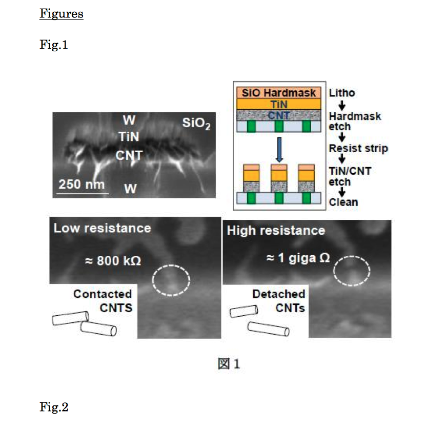
NRAM is being developed by Nantero as a candidate for next generation non-volatile memory. It operates On/Off switching by touch (low resistance) / detach (high resistance) of carbon nanotubes triggered by voltage/current pulses (Figs.1, 3). A schematic of the memory array (Fig. 2) illustrates 1T-1R cells, with a MOSFET select device and a NV carbon nanotube (CNT) resistive storage element per cell, and driver and sense amplifier/buffer supporting circuits. The proposed method, which is stable against dispersion and fluctuation in the NRAM memory array, achieves high speed (20ns write pulse) and low current (less than 20 uA) On/Off state switching (Fig.3) with more than 100 times resistance change after switching (Fig.4). The magnitude of the resistance change of NRAM memory cells is big enough to show that NRAM can support stable multi-bit memory operation in a single memory cell i.e. multi-level cell (MLC) operation, which is suitable for larger capacity memory devices. Greater than 10E11 Set and Reset cycle endurance is feasible (Fig.5). The use of Flash memory has been limited to data storage only because of its limited Set & Reset cycle endurance, whereas NRAM, which has one million times better cycle endurance can potentially replace DRAM, in addition to its application as data storage.
This work is based on early stage NRAM devices having a relatively large cell size (140nm) with single bit memory storage. Further work is needed with statistical data evaluation before NRAM can be productized as Gigabit level memory devices. However, even though this work is in early stages, the performance and reliability of NRAM shown here is excellent enough to demonstrate that NRAM is a viable technology to implement as ‘universal memory’ which could potentially replace both main memory (DRAM) and storage memory (HDD, SSD) in the future, and contribute to higher performance, lower power and more robust IT systems in our society.


